

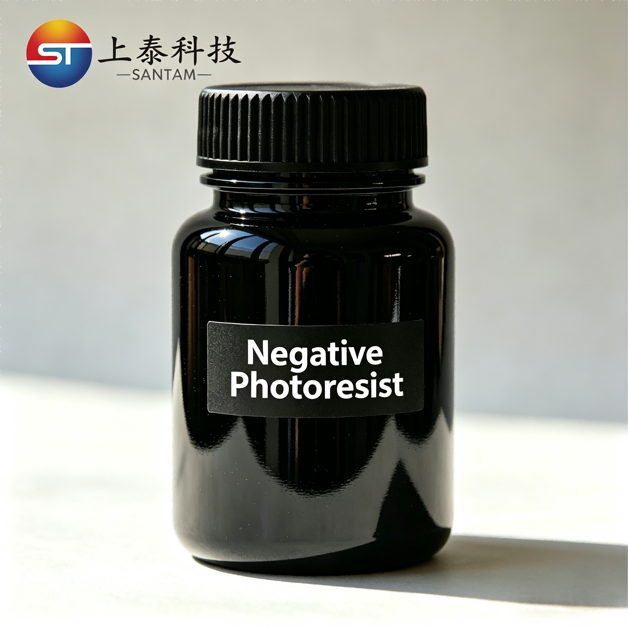
Negative Photoresist
Product overview
A cross-linking reaction occurs in the exposed area and is insoluble in the developer, forming a negative image pattern. It has good etching resistance and electroplating resistance, and is widely used in integrated circuits, advanced packaging and microelectromechanical systems (MEMS) manufacturing processes.
Core features
- High sensitivity
- Excellent line width control
- Good adhesion
- Low defect density
Application areas
- Semiconductor packaging
- MEMS device
- Advanced packaging
- Wafer level packaging
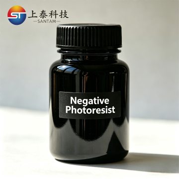
Product pictures