




Breaking the Technical Boundary: Santam Technology's Photoresist Solution Empowers Precision Manufacturing in Multiple Industries
In this era of rapid technological advancement, photoresist, as a critical material for micro-pattern processing, is driving innovative breakthroughs in fields such as semiconductors, display panels, and new energy. Chengdu Santam Technology Co., Ltd. leverages its comprehensive photoresist product line to provide customized solutions for various industries, propelling precision manufacturing to new heights.
Multiple technical approaches to meet varying precision requirements
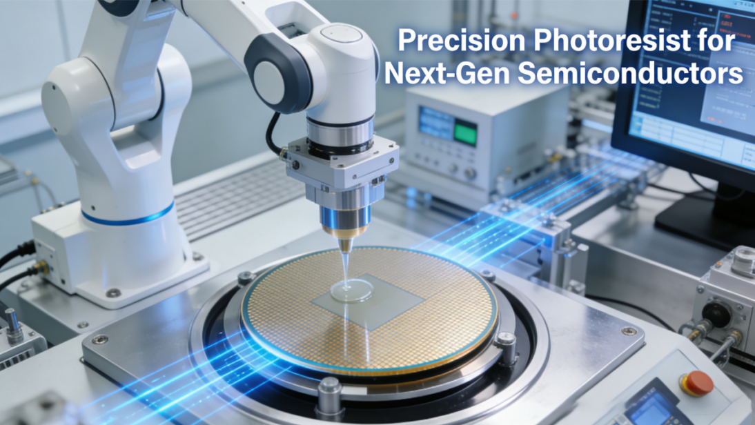
Santam Technology's photoresist products span both positive and negative technology routes, covering the full wavelength range from G-line (436nm) to extreme ultraviolet (EUV, 13.5nm). Positive photoresists excel in advanced semiconductor processes, with ArF photoresists supporting 20-90nm resolution for FinFET and 3D NAND technologies. Negative photoresists, meanwhile, demonstrate unique advantages in thick-film processing, enabling microstructures with a deep-to-width ratio of up to 50:1 to meet the demands of MEMS and high-end sensor manufacturing.
Semiconductor Manufacturing: From Mature Process to Cutting-edge Process
In the semiconductor industry, Santam Technology's product portfolio comprehensively addresses diverse process requirements. Its G-line/I-line positive resists are designed for mature processes above 0.35μm, KrF positive resists for critical layers in 90-180nm nodes, and ArF positive resists for 28-7nm advanced processes. For cutting-edge processes below 5nm, the company's EUV photoresist solutions demonstrate exceptional resolution performance.
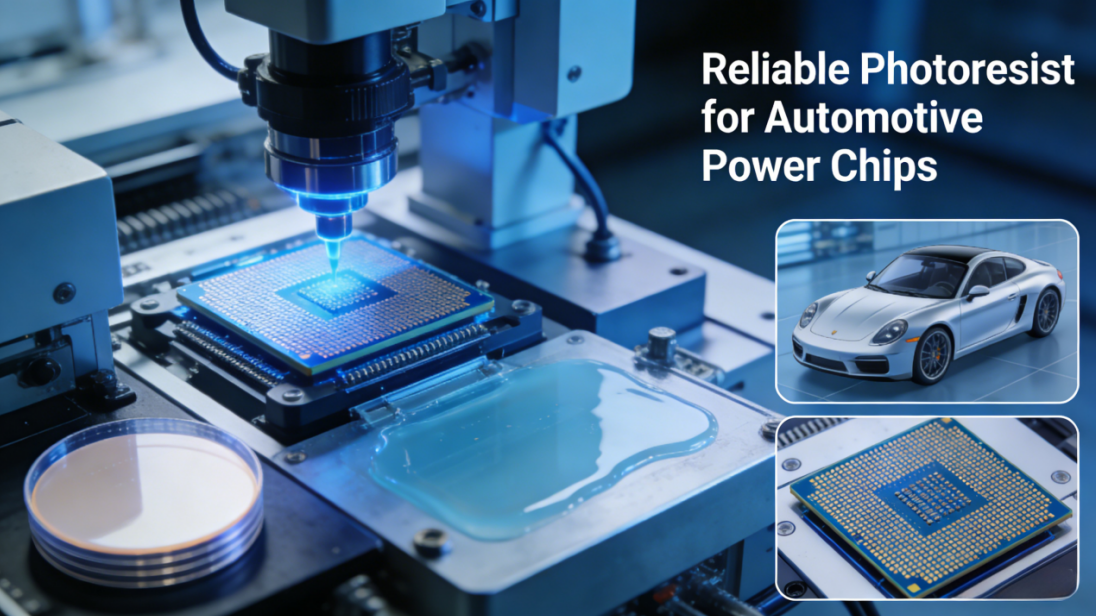
In advanced packaging, Santam Technology's photoresist demonstrates exceptional performance in wafer-level packaging (WLP) and system-level packaging (SiP), providing reliable patterning support for critical processes including redistribution layers (RDL) and through-silicon vias (TSV).
Display Panel: Driving LCD and OLED Technology Innovation
For the display industry, Santam Technology provides specially optimized photoresist solutions. In LCD manufacturing, the company's products are used in critical processes such as black matrix (BM), RGB color resist, and TFT arrays. In the OLED field, its pixel definition layer (PDL) photoresist supports high-precision patterning, enhancing pixel density and yield.
New Energy and Advanced Manufacturing:Expanding the Application Boundary
In the photovoltaic sector, Santam Technology's photoresist is utilized in the patterning processes of high-efficiency cell technologies including PERC, TOPCon, and HJT, providing critical material support for the renewable energy industry. Additionally, the company's solutions in fields such as PCB/FPC, optical communications, and microwave devices demonstrate outstanding performance and adaptability.
Continuous innovation leads the development of the industry
Chengdu Santam Technology Co., Ltd. is dedicated to the R&D and innovation of photoresist technology. By continuously refining its product portfolio and advancing technical capabilities, the company provides customers with superior and precise solutions. Going forward, it will deepen collaborations with partners across industries to jointly drive the advancement of precision manufacturing technologies.