









Breakthrough in Photoresist Technology! Chengdu Santam Technology Deeply Layouts the Whole Industry Chain of Semiconductor, Display and New Energy
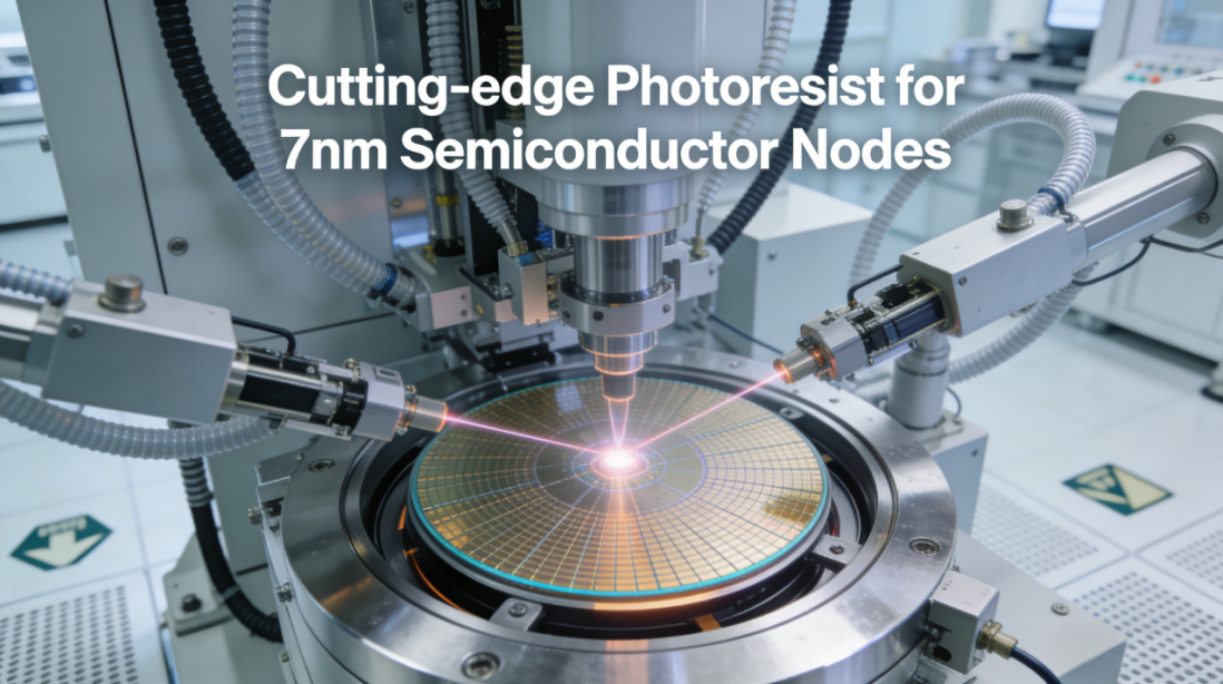
As the global semiconductor industry accelerates toward advanced manufacturing processes and the display panel and photovoltaic industries experience rapid growth both domestically and internationally, photoresist—this core material in microelectronics manufacturing—is witnessing unprecedented market opportunities. Leveraging its deep expertise in polyurea and specialty chemicals, Chengdu Santam Technology Co., Ltd. has been driving innovation in photoresist application technologies, delivering comprehensive solutions for key sectors including semiconductors, LCD/OLED displays, PCBs, and photovoltaics.

- Positive Photoresist: Full Coverage from Mature Process to Advanced Process
In semiconductor manufacturing, positive photoresists have become indispensable key materials for wafer fabrication due to their high resolution and superior pattern transfer capability. According to Chengdu Santam Technology's technical team, the company's full-spectrum positive photoresists covering G-line (436nm) to EUV (13.5nm) can meet the differentiated requirements of various process nodes.
- I-line positive photoresist (365nm): Widely used in mature 0.35-0.8μm processes, LCD black matrix (BM)/RGB color resist, and MEMS sensor manufacturing, demonstrating outstanding performance in TFT-LCD array substrates and inertial sensor microstructures.
- KrF positive photoresist (248nm): Supports critical logic/storage layers (90-180nm) and plays a pivotal role in advanced packaging technologies such as interlayer dielectric patterning and wafer-level packaging (WLP) redistribution layers (RDL) for 3D NAND flash memory.
- ArF positive photoresist (193nm): Designed for advanced processes including 28-7nm FinFET and 3D NAND gate/through-hole, it supports the development of domestically produced advanced logic chips.
- EUV positive photoresist (13.5nm): Overcoming the technological bottleneck of 7nm and below, it establishes core material capabilities for next-generation chip technology.
"In the MEMS sensor industry, our positive thick film adhesive achieves needle-free coating with 3-15μm thickness, maintains high pattern fidelity for over 2 hours under deep silicon etching (KOH wet etching), and eliminates drilling and collapse issues," stated a representative from Chengdu Santam Technology. "This innovation holds significant substitution value in both domestic and international high-end MEMS manufacturing supply chains."
- Negative Photoresist: Core Support for High Aspect Ratio Structures and Advanced Packaging
Negative photoresists demonstrate irreplaceable advantages in MEMS microstructures, advanced packaging, and power devices due to their exceptional etch resistance and high aspect ratio formation capability. Chengdu Santam Technology has achieved breakthroughs in developing the cyclodized rubber-diazide system and chemically amplified resist (CAR-N) negative photoresist, which include the following advancements:
| application area | Core technical indicators | artificial value |
| MEMS high aspect ratio structure | The aspect ratio can reach 50:1, with a film thickness of 5-100 μm. | Pressure sensor diaphragm, inertial sensor mass block, microfluidic chip channel |
| Wafer Level Packaging (WLP) | Resistant to electroplating with copper/tin, withstands 260°C reflow soldering | Bump fabrication and TSV insulating layer patterning |
| Power devices (SiC/GaN) | Metal vapor deposition resistant to 300℃ and compatible with compound semiconductors | Lift-off Process of RF Device Electrode and Mask for MOSFET Gate Oxide |
| 3D NAND/Advanced Logic | Resolution of 30nm (EUV negative photoresist) | Advanced isolation layer and patterned hard mask for 5nm and below processes |
In third-generation semiconductor applications like SiC power devices and GaN RF components, the company's negative adhesive has achieved excellent compatibility with GaN epitaxial wafers. It ensures sharp edges without lateral etching and eliminates metal residue after 5 minutes of acetone ultrasonic stripping, significantly improving the yield rate in compound semiconductor manufacturing.
- Display and Photovoltaic: A New Growth Pole of Photoresist Application
LCD/OLED display manufacturing
In the display panel industry, photoresist applications are expanding beyond traditional array substrate processes to include emerging display technologies such as flexible OLED and Mini/Micro LED.
- LCD color film (CF) manufacturing: The carbon black dispersion-based black positive photoresist achieves low light transmittance (<0.1%) with ±2μm line width precision and effective light leakage prevention; the RGB color-blocking photoresist delivers NTSC ≥95% color purity.
- OLED pixel definition layer (PDL): The negative pixel definition photoresist features ±1μm opening precision, is solvent-resistant, and its low shrinkage ensures precise evaporation.
- Flexible displays: Photosensitive polyimide (PSPI) photoresist with over 10^4-fold bending resistance, compatible with foldable screen thin film encapsulation (TFE) and flexible substrate insulation layers.
photovoltaic cell manufacturing
With the rapid adoption of N-type TOPCon and HJT heterojunction cell technologies, the demand for photoresists in the photovoltaic industry has surged dramatically.
- N-type TOPCon solar cells: The I-line positive electrode achieves high-resolution patterning (line width ≤50μm) in the polysilicon doped region, exhibits strong adhesion to the SiO₂ passivation layer, and demonstrates resistance to ion implantation.
- HJT cell: Low-temperature curing positive photoresist (≤200℃) is compatible with ITO/ZnO thin-film patterning, while Lift-off negative photoresist (PMMA-based) enables silver paste grid lines with inverted trapezoidal profiles, achieving complete residue-free peeling.
- Perovskite solar cells: Flexible UV-curable negative photoresist (polyurethane acrylate) with low-temperature compatibility (≤150°C) and solvent-free properties, paving the way for the industrialization of next-generation thin-film photovoltaic technology.
- Technological Prospects: Synergistic Innovation of Polyurea Materials and Photoresist
As a polyurea manufacturer, Chengdu Santam Technology is exploring innovative applications of polyurea materials in the photoresist field. Polyurea materials exhibit excellent chemical corrosion resistance, mechanical strength, and thermal stability, with potential breakthroughs expected in the following areas:
- Photoresist resin modification: Utilizing the rigid chain segments of polyurea to enhance the etching resistance and thermal stability of photoresist;
- Thick-film photoresist system: Develop high aspect ratio negative photoresist based on polyurea cross-linked network to meet the extreme process requirements of MEMS and advanced packaging.
- Functional coatings: These provide additional protective or planarization layers for photoresists, enhancing the reliability of multilayer patterning processes.
epilogue
Facing the historic opportunity of global semiconductor material supply chain restructuring, Chengdu Santam Technology Co., Ltd. will continue to increase R&D investment, deepen strategic cooperation with downstream wafer fabs, panel manufacturers, and photovoltaic enterprises, and promote continuous breakthroughs in key indicators such as resolution, sensitivity, and etching resistance for domestic photoresists, contributing to the self-reliance and controllability of China's high-end manufacturing industry.
About Chengdu Santam Technology Co., Ltd.
Chengdu Santam Technology Co., Ltd. is a high-tech enterprise specializing in the R&D, production, and sales of polyurea and specialty chemicals. Its products are widely used in coatings, adhesives, electronic materials, and related fields. Leveraging its strong technological innovation capabilities, the company is actively expanding into strategic emerging industries such as semiconductors, displays, and new energy, with the goal of becoming a world-class provider of functional materials solutions.
For more information about photoresist products or technical collaboration, please visit Chengdu Santam Technology's official website or contact our technical team.